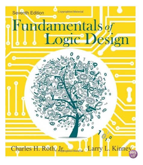
Instant download Solution Manual for Fundamentals of Logic Design 7th Edition by Roth pdf docx epub after payment.

Product details:
- ISBN-10 : 1133628478
- ISBN-13 : 978-1133628477
- Author:
Updated with modern coverage, a streamlined presentation, and excellent companion software, this seventh edition of FUNDAMENTALS OF LOGIC DESIGN achieves yet again an unmatched balance between theory and application. Authors Charles H. Roth, Jr. and Larry L. Kinney carefully present the theory that is necessary for understanding the fundamental concepts of logic design while not overwhelming students with the mathematics of switching theory. Divided into 20 easy-to-grasp study units, the book covers such fundamental concepts as Boolean algebra, logic gates design, flip-flops, and state machines. By combining flip-flops with networks of logic gates, students will learn to design counters, adders, sequence detectors, and simple digital systems. After covering the basics, this text presents modern design techniques using programmable logic devices and the VHDL hardware description language.
Table of contents:
- UNIT 1. INTRODUCTION NUMBER SYSTEMS AND CONVERSION
- 1.1. Digital Systems and Switching Circuits
- 1.2. Number Systems and Conversion
- 1.3. Binary Arithmetic
- 1.4. Representation of Negative Numbers
- Sign and Magnitude Numbers
- 2’s Complement Numbers
- Addition of 2’s Complement Numbers
- 1’s Complement Numbers
- Addition of 1’s Complement Numbers
- 1.5. Binary Codes
- Problems
- UNIT 2. BOOLEAN ALGEBRA
- 2.1. Introduction
- 2.2. Basic Operations
- 2.3. Boolean Expressions and Truth Tables
- 2.4. Basic Theorems
- 2.5. Commutative, Associative, Distributive, and DeMorgan’s Laws
- 2.6. Simplification Theorems
- 2.7. Multiplying Out and Factoring
- 2.8. Complementing Boolean Expressions
- Problems
- UNIT 3. BOOLEAN ALGEBRA (CONTINUED)
- 3.1. Multiplying Out and Factoring Expressions
- 3.2. Exclusive-OR and Equivalence Operations
- 3.3. The Consensus Theorem
- 3.4. Algebraic Simplification of Switching Expressions
- 3.5. Proving Validity of an Equation
- Programmed Exercise 3.1
- Programmed Exercise 3.2
- Programmed Exercise 3.3
- Programmed Exercise 3.4
- Programmed Exercise 3.5
- Problems
- UNIT 4. APPLICATIONS OF BOOLEAN ALGEBRA MINTERM AND MAXTERM EXPANSIONS
- 4.1. Conversion of English Sentences to Boolean Equations
- 4.2. Combinational Logic Design Using a Truth Table
- 4.3. Minterm and Maxterm Expansions
- 4.4. General Minterm and Maxterm Expansions
- 4.5. Incompletely Specified Functions
- 4.6. Examples of Truth Table Construction
- 4.7. Design of Binary Adders and Subtracters
- Problems
- UNIT 5. KARNAUGH MAPS
- 5.1. Minimum Forms of Switching Functions
- 5.2. Two- and Three-Variable Karnaugh Maps
- 5.3. Four-Variable Karnaugh Maps
- 5.4. Determination of Minimum Expressions Using Essential Prime Implicants
- 5.5. Five-Variable Karnaugh Maps
- 5.6. Other Uses of Karnaugh Maps
- 5.7. Other Forms of Karnaugh Maps
- Programmed Exercise 5.1
- Programmed Exercise 5.2
- Problems
- UNIT 6. QUINE-MCCLUSKEY METHOD
- 6.1. Determination of Prime Implicants
- 6.2. The Prime Implicant Chart
- 6.3. Petrick’s Method
- 6.4. Simplification of Incompletely Specified Functions
- 6.5. Simplification Using Map-Entered Variables
- 6.6. Conclusion
- Programmed Exercise 6.1
- Problems
- UNIT 7. MULTI-LEVEL GATE CIRCUITS NAND AND NOR GATES
- 7.1. Multi-Level Gate Circuits
- 7.2. NAND and NOR Gates
- 7.3. Design of Two-Level NAND- and NOR-Gate Circuits
- 7.4. Design of Multi-Level NAND- and NOR-Gate Circuits
- 7.5. Circuit Conversion Using Alternative Gate Symbols
- 7.6. Design of Two-Level, Multiple-Output Circuits
- Determination of Essential Prime Implicants for Multiple-Output Realization
- 7.7. Multiple-Output NAND- and NOR-Gate Circuits
- Problems
- UNIT 8. COMBINATIONAL CIRCUIT DESIGN AND SIMULATION USING GATES
- 8.1. Review of Combinational Circuit Design
- 8.2. Design of Circuits with Limited Gate Fan-In
- 8.3. Gate Delays and Timing Diagrams
- 8.4. Hazards in Combinational Logic
- 8.5. Simulation and Testing of Logic Circuits
- Problems
- Design Problems
- UNIT 9. MULTIPLEXERS, DECODERS, AND PROGRAMMABLE LOGIC DEVICES
- 9.1. Introduction
- 9.2. Multiplexers
- 9.3. Three-State Buffers
- 9.4. Decoders and Encoders
- 9.5. Read-Only Memories
- 9.6. Programmable Logic Devices
- Programmable Logic Arrays
- Programmable Array Logic
- 9.7. Complex Programmable Logic Devices
- 9.8. Field-Programmable Gate Arrays
- Decomposition of Switching Functions
- Problems
- UNIT 10. INTRODUCTION TO VHDL
- 10.1. VHDL Description of Combinational Circuits
- 10.2. VHDL Models for Multiplexers
- 10.3. VHDL Modules
- Four-Bit Full Adder
- 10.4. Signals and Constants
- 10.5. Arrays
- 10.6. VHDL Operators
- 10.7. Packages and Libraries
- 10.8. IEEE Standard Logic
- 10.9. Compilation and Simulation of VHDL Code
- Problems
- Design Problems
- UNIT 11. LATCHES AND FLIP-FLOPS
- 11.1. Introduction
- 11.2. Set-Reset Latch
- 11.3. Gated Latches
- 11.4. Edge-Triggered D Flip-Flop
- 11.5. S-R Flip-Flop
- 11.6. J-K Flip-Flop
- 11.7. T Flip-Flop
- 11.8. Flip-Flops with Additional Inputs
- 11.9. Asynchronous Sequential Circuits
- 11.10. Summary
- Problems
- Programmed Exercise 11.35
- UNIT 12. REGISTERS AND COUNTERS
- 12.1. Registers and Register Transfers
- Parallel Adder with Accumulator
- 12.2. Shift Registers
- 12.3. Design of Binary Counters
- 12.4. Counters for Other Sequences
- Counter Design Using D Flip-Flops
- 12.5. Counter Design Using S-R and J-K Flip-Flops
- 12.6. Derivation of Flip-Flop Input Equations—Summary
- Problems
- 12.1. Registers and Register Transfers
- UNIT 13. ANALYSIS OF CLOCKED SEQUENTIAL CIRCUITS
- 13.1. A Sequential Parity Checker
- 13.2. Analysis by Signal Tracing and Timing Charts
- 13.3. State Tables and Graphs
- Construction and Interpretation of Timing Charts
- 13.4. General Models for Sequential Circuits
- Programmed Exercise 13.1
- Problems
- UNIT 14. DERIVATION OF STATE GRAPHS AND TABLES
- 14.1. Design of a Sequence Detector
- 14.2. More Complex Design Problems
- 14.3. Guidelines for Construction of State Graphs
- 14.4. Serial Data Code Conversion
- 14.5. Alphanumeric State Graph Notation
- 14.6. Incompletely Specified State Tables
- Programmed Exercise 14.1
- Programmed Exercise 14.2
- Programmed Exercise 14.3
- Problems
- UNIT 15. REDUCTION OF STATE TABLES STATE ASSIGNMENT
- 15.1. Elimination of Redundant States
- 15.2. Equivalent States
- 15.3. Determination of State Equivalence Using an Implication Table
- 15.4. Equivalent Sequential Circuits
- 15.5. Reducing Incompletely Specified State Tables
- 15.6. Derivation of Flip-Flop Input Equations
- 15.7. Equivalent State Assignments
- 15.8. Guidelines for State Assignment
- 15.9. Using a One-Hot State Assignment
- Problems
- UNIT 16. SEQUENTIAL CIRCUIT DESIGN
- 16.1. Summary of Design Procedure for Sequential Circuits
- 16.2. Design Example—Code Converter
- 16.3. Design of Iterative Circuits
- Design of a Comparator
- 16.4. Design of Sequential Circuits Using ROMs and PLAs
- 16.5. Sequential Circuit Design Using CPLDs
- 16.6. Sequential Circuit Design Using FPGAs
- 16.7. Simulation and Testing of Sequential Circuits
- 16.8. Overview of Computer-Aided Design
- Design Problems
- Additional Problems
- UNIT 17. VHDL FOR SEQUENTIAL LOGIC
- 17.1. Modeling Flip-Flops Using VHDL Processes
- 17.2. Modeling Registers and Counters Using VHDL Processes
- 17.3. Modeling Combinational Logic Using VHDL Processes
- 17.4. Modeling a Sequential Machine
- 17.5. Synthesis of VHDL Code
- 17.6. More About Processes and Sequential Statements
- Problems
- Simulation Problems
- UNIT 18. CIRCUITS FOR ARITHMETIC OPERATIONS
- 18.1. Serial Adder with Accumulator
- 18.2. Design of a Binary Multiplier
- 18.3. Design of a Binary Divider
- Programmed Exercise 18.1
- Programmed Exercise 18.2
- Problems
- UNIT 19. STATE MACHINE DESIGN WITH SM CHARTS
- 19.1. State Machine Charts
- 19.2. Derivation of SM Charts
- 19.3. Realization of SM Charts
- Problems
- UNIT 20. VHDL FOR DIGITAL SYSTEM DESIGN
- 20.1. VHDL Code for a Serial Adder
- 20.2. VHDL Code for a Binary Multiplier
- 20.3. VHDL Code for a Binary Divider
- 20.4. VHDL Code for a Dice Game Simulator
- 20.5. Concluding Remarks
- Problems
- Lab Design Problems
- APPENDIX A. MOS AND CMOS LOGIC
- APPENDIX B. VHDL LANGUAGE SUMMARY
- APPENDIX C. TIPS FOR WRITING SYNTHESIZABLE VHDL CODE
- APPENDIX D. PROOFS OF THEOREMS
- REFERENCES
People also search:
Fundamentals of Logic Design 7th Edition
Fundamentals of Logic Design 7th Edition pdf
Fundamentals of Logic Design
fundamentals of digital logic and design
fundamentals of digital logic and microcomputer design


