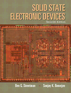
Instant download Solutions Manual for Solid State Electronic Devices 7e by Ben Streetman 0133356035 pdf docx epub after payment.

Product details:
- ISBN-10 : 0133356035
- ISBN-13 : 978-0133356038
- Author: Ben G. Streetman; Sanjay Kumar Banerjee
One of the most widely used introductory books on semiconductor materials, physics, devices and technology, Solid State Electronic Devices aims to: 1) develop basic semiconductor physics concepts, so students can better understand current and future devices; and 2) provide a sound understanding of current semiconductor devices and technology, so that their applications to electronic and optoelectronic circuits and systems can be appreciated. Students are brought to a level of understanding that will enable them to read much of the current literature on new devices and applications.
Table of contents:
ABOUT THE AUTHORS XvII
1 CRYSTAL PROPERTIES AND GROWTH
OF SEMICONDUCTORS 1
1.1 Semiconductor Materials 1
1.2 Crystal Lattices 3
1.3 Bulk Crystal Growth 12
1.4 epitaxial Growth 17
1.2.1 Periodic Structures 3
1.2.2 Cubic Lattices 5
1.2.3 Planes and directions 7
1.2.4 The diamond Lattice 9
1.3.1 Starting Materials 12
1.3.2 Growth of Single-Crystal Ingots 13
1.3.3 wafers 14
1.3.4 doping 16
1.4.1 Lattice-Matching in epitaxial Growth 17
1.4.2 vapor-Phase epitaxy 19
1.4.3 Molecular Beam epitaxy 22
1.5 wave Propagation in discrete, Periodic Structures 24
2 ATOMS AND ELECTRONS 32
2.1 Introduction to Physical Models 33
2.2 experimental Observations 34
2.3 The Bohr Model 37
2.4 Quantum Mechanics 41
2.2.1 The Photoelectric effect 34
2.2.2 Atomic Spectra 36
2.5 Atomic Structure and the Periodic Table 49
2.4.1 Probability and the Uncertainty Principle 41
2.4.2 The Schrödinger wave equation 43
2.4.3 Potential well Problem 45
2.4.4 Tunneling 48
2.5.1 The hydrogen Atom 50
2.5.2 The Periodic Table 52
3 ENERGY BANDS AND CHARGE CARRIERS IN SEMICONDUCTORS 63
3.1 Bonding Forces and energy Bands in Solids 63
3.2 Charge Carriers in Semiconductors 74
3.3 Carrier Concentrations 89
3.4 drift of Carriers in electric and Magnetic Fields 100
3.1.1 Bonding Forces in Solids 64
3.1.2 energy Bands 66
3.1.3 Metals, Semiconductors, and Insulators 69
3.1.4 direct and Indirect Semiconductors 70
3.1.5 variation of energy Bands with Alloy Composition 72
3.2.1 electrons and holes 74
3.2.2 effective Mass 79
3.2.3 Intrinsic Material 83
3.2.4 extrinsic Material 84
3.2.5 electrons and holes in Quantum wells 87
3.3.1 The Fermi Level 89
3.3.2 electron and hole Concentrations at equilibrium 92
3.3.3 Temperature dependence of Carrier Concentrations 97
3.3.4 Compensation and Space Charge neutrality 99
3.4.1 Conductivity and Mobility 100
3.4.2 drift and Resistance 105
3.4.3 effects of Temperature and doping on Mobility 106
3.4.4 high-Field effects 109
3.4.5 The hall effect 109
3.5 Invariance of the Fermi Level at equilibrium 111
4 EXCESS CARRIERS IN SEMICONDUCTORS 122
4.1 Optical Absorption 122
4.2 Luminescence 125
4.3 Carrier Lifetime and Photoconductivity 128
4.4 diffusion of Carriers 137
4.2.1 Photoluminescence 126
4.2.2 electroluminescence 128
4.3.1 direct Recombination of electrons and holes 129
4.3.2 Indirect Recombination; Trapping 131
4.3.3 Steady State Carrier Generation; Quasi-Fermi Levels 134
4.3.4 Photoconductive devices 136
4.4.1 diffusion Processes 138
4.4.2 diffusion and drift of Carriers; Built-in Fields 140
4.4.3 diffusion and Recombination; The Continuity equation 143
4.4.4 Steady State Carrier Injection; diffusion Length 145
4.4.5 The haynes–Shockley experiment 147
4.4.6 Gradients in the Quasi-Fermi Levels 150
5 JUNCTIONS159
5.1 Fabrication of p-n Junctions 159
5.2 equilibrium Conditions 174
5.3 Forward- and Reverse-Biased
5.4 Reverse-Bias Breakdown 200
5.5 Transient and A-C Conditions 209
5.6 deviations from the Simple Theory 222
5.7 Metal–Semiconductor Junctions 231
5.1.1 Thermal Oxidation 160
5.1.2 diffusion 161
5.1.3 Rapid Thermal Processing 163
5.1.4 Ion Implantation 164
5.1.5 Chemical vapor deposition (Cvd) 167
5.1.6 Photolithography 168
5.1.7 etching 171
5.1.8 Metallization 173
5.2.1 The Contact Potential 175
5.2.2 equilibrium Fermi Levels 180
5.2.3 Space Charge at a Junction 180
Junctions; Steady State Conditions 185
5.3.1 Qualitative description of Current Flow at a Junction 185
5.3.2 Carrier Injection 189
5.3.3 Reverse Bias 198
5.4.1 Zener Breakdown 201
5.4.2 Avalanche Breakdown 202
5.4.3 Rectifiers 205
5.4.4 The Breakdown diode 208
5.5.1 Time variation of Stored Charge 209
5.5.2 Reverse Recovery Transient 212
5.5.3 Switching diodes 216
5.5.4 Capacitance of p-n Junctions 216
5.5.5 The varactor diode 221
5.6.1 effects of Contact Potential on Carrier Injection 223
5.6.2 Recombination and Generation in the Transition Region 225
5.6.3 Ohmic Losses 227
5.6.4 Graded Junctions 228
5.7.1 Schottky Barriers 231
5.7.2 Rectifying Contacts 233
5.7.3 Ohmic Contacts 235
5.7.4 Typical Schottky Barriers 237
5.8 heterojunctions 238
6 FIELD-EFFECT TRANSISTORS 257
6.1 Transistor Operation 258
6.2 The Junction FeT 260
6.3 The Metal—Semiconductor FeT 267
6.4 The Metal—Insulator—Semiconductor FeT 271
6.5 The MOS Field-effect Transistor 299
6.6 Advanced MOSFeT Structures 330
6.1.1 The Load Line 258
6.1.2 Amplification and Switching 259
6.2.1 Pinch-off and Saturation 261
6.2.2 Gate Control 263
6.2.3 Current—voltage Characteristics 265
6.3.1 The GaAs MeSFeT 267
6.3.2 The high electron Mobility Transistor (heMT) 268
6.3.3 Short Channel effects 270
6.4.1 Basic Operation and Fabrication 271
6.4.2 The Ideal MOS Capacitor 275
6.4.3 effects of Real Surfaces 286
6.4.4 Threshold voltage 289
6.4.5 MOS Capacitance—voltage Analysis 291
6.4.6 Time-dependent Capacitance Measurements 295
6.4.7 Current—voltage Characteristics of MOS Gate Oxides 296
6.5.1 Output Characteristics 299
6.5.2 Transfer Characteristics 302
6.5.3 Mobility Models 305
6.5.4 Short Channel MOSFeT I—V Characteristics 307
6.5.5 Control of Threshold voltage 309
6.5.6 Substrate Bias effects–the “body” effect 312
6.5.7 Subthreshold Characteristics 316
6.5.8 equivalent Circuit for the MOSFeT 318
6.5.9 MOSFeT Scaling and hot electron effects 321
6.5.10 drain-Induced Barrier Lowering 325
6.5.11 Short Channel effect and narrow width effect 327
6.5.12 Gate-Induced drain Leakage 329
6.6.1 Metal Gate-high-k 330
6.6.2 enhanced Channel Mobility Materials and Strained Si FeTs 331
6.6.3 SOI MOSFeTs and FinFeTs 333
7 BIPOLAR JUNCTION TRANSISTORS 348
7.1 Fundamentals of BJT Operation 348
7.2 Amplification with BJTs 352
7.3 BJT Fabrication 355
7.4 Minority Carrier distributions and Terminal Currents 358
7.5 Generalized Biasing 367
7.6 Switching 375
7.7 Other Important effects 380
7.8 Frequency Limitations of Transistors 394
7.4.1 Solution of the diffusion equation in the Base Region 359
7.4.2 evaluation of the Terminal Currents 361
7.4.3 Approximations of the Terminal Currents 364
7.4.4 Current Transfer Ratio 366
7.5.1 The Coupled-diode Model 368
7.5.2 Charge Control Analysis 373
7.6.1 Cutoff 376
7.6.2 Saturation 377
7.6.3 The Switching Cycle 378
7.6.4 Specifications for Switching Transistors 379
7.7.1 drift in the Base Region 381
7.7.2 Base narrowing 382
7.7.3 Avalanche Breakdown 383
7.7.4 Injection Level; Thermal effects 385
7.7.5 Base Resistance and emitter Crowding 386
7.7.6 Gummel—Poon Model 388
7.7.7 Kirk effect 391
7.8.1 Capacitance and Charging Times 394
7.8.2 Transit Time effects 397
7.8.3 webster effect 398
7.8.4 high-Frequency Transistors 398
7.9 heterojunction Bipolar Transistors 400
8 OPTOELECTRONIC DEVICES 410
8.1 Photodiodes 410
8.1.1 Current and voltage in an Illuminated Junction 411
8.1.2 Solar Cells 414
8.1.3 Photodetectors 417
8.1.4 Gain, Bandwidth, and Signal-to-noise Ratio
of Photodetectors 419
8.2 Light-emitting diodes 422
8.3 Lasers 430
8.4 Semiconductor Lasers 434
8.2.1 Light-emitting Materials 423
8.2.2 Fiber-Optic Communications 427
8.4.1 Population Inversion at a Junction 435
8.4.2 emission Spectra for p-n Junction Lasers 437
8.4.3 The Basic Semiconductor Laser 438
8.4.4 heterojunction Lasers 439
8.4.5 Materials for Semiconductor Lasers 442
8.4.6 Quantum Cascade Lasers 444
9 INTEGRATED CIRCUITS 452
9.1 Background 453
9.2 evolution of Integrated Circuits 456
9.3 Monolithic device elements 459
9.1.1 Advantages of Integration 453
9.1.2 Types of Integrated Circuits 455
9.4 Charge Transfer devices 480
9.5 Ultra Large-Scale Integration (ULSI) 485
9.6 Testing, Bonding, and Packaging 510
9.3.1 CMOS Process Integration 459
9.3.2 Integration of Other Circuit elements 474
9.4.1 dynamic effects in MOS Capacitors 481
9.4.2 The Basic CCd 482
9.4.3 Improvements on the Basic Structure 483
9.4.4 Applications of CCds 484
9.5.1 Logic devices 489
9.5.2 Semiconductor Memories 497
9.6.1 Testing 511
9.6.2 wire Bonding 511
9.6.3 Flip-Chip Techniques 515
9.6.4 Packaging 515
10 HIGH-FREQUENCY, HIGH-POWER AND
NANOELECTRONIC DEVICES 521
10.1 Tunnel diodes 521
10.2 The IMPATT diode 525
10.3 The Gunn diode 528
10.1.1 degenerate Semiconductors 521
10.3.1 The Transferred-electron Mechanism 528
10.3.2 Formation and drift of Space Charge domains 531
10.4 The p-n-p-n diode 533
10.5 The Semiconductor-Controlled Rectifier 539
10.6 Insulated-Gate Bipolar Transistor 541
10.7 nanoelectronic devices 544
10.4.1 Basic Structure 533
10.4.2 The Two-Transistor Analogy 534
10.4.3 variation of a with Injection 535
10.4.4 Forward-Blocking State 536
10.4.5 Conducting State 537
10.4.6 Triggering Mechanisms 538
10.5.1 Turning off the SCR 540
10.7.1 Zero-dimensional Quantum dots 544
10.7.2 One-dimensional Quantum wires 546
10.7.3 Two-dimensional Layered Crystals 547
10.7.4 Spintronic Memory 548
10.7.5 nanoelectronic Resistive Memory 550
AppendIces
I. definitions of Commonly Used Symbols 555
II. Physical Constants and Conversion Factors 559
III. Properties of Semiconductor Materials 560
Iv. derivation of the density of States in the Conduction
v. derivation of Fermi—dirac Statistics 566
vI. dry and wet Thermal Oxide Thickness Grown on
vII. Solid Solubilities of Impurities in Si 571
vIII. diffusivities of dopants in Si and SiO2 572
IX. Projected Range and Straggle as Function of Implant
Answers to Selected Self Quiz Questions 576
Index 581
Band 561
Si (100) as a Function of Time and Temperature 569
energy in Si 574
People also search:
Solid State Electronic Devices 7e
Solid State Electronic Devices 7e pdf
Solid State Electronic Devices
|
why are solid-state electronic devices so named |


